Archive for the 'Technology' Category
Looking for the building block of the universe

The European Organization for Nuclear Research commonly known as CERN is located in Geneva and using the world’s powerful equipment known as the Large Hadron Collider conduct research on particle acceleration. The 17 mile long circular path for the collider can run 11,000 laps per second, very much close to the speed of light. It cost $6.6 billion to build and took more than 10 years to complete. It has an annual budget of $1.3 billion. It started its operations in 2008 and currently undergoing $105 million upgrade. The next phase of research is planned to start in March 2015. It is expected to unravel mysteries of the universe through its research, primarily by colliding atoms.
A new director is scheduled to take over operations of CERN in January 2016 and she is working hard to recruit new member countries to reduce the financial burden on current members. Most of its members are from Europe and Israel joined the organization last year as a full member. The scientists of the CERN are looking for the building block of the universe that vanished after the big bang. The organization uses its own software to analyze data they collect.
No commentsSofter and gentle robots are coming soon
Rough and rigid robotic arms were not only unable to handle delicate work but also disliked by many. This is why new breed of developers including Empire Robotics and Pneubotics are developing much softer arms. They don’t have electronics components but still grip delicate items such as a bulb due to softer grip connected to a hard robot. Some are even testing pumped air into the robotic arm to provider softer touch. Vinyl material containing veins that hold air, water and hydraulic fluids that work like muscles are connected to motors instead of more rigid parts to provide the softer touch.
New breed of robotic companies are working on gently handling sick patients, pull bricks at a disaster site to save an injured person, and even safely place an elderly on a bed. The United States government is also supporting some of these efforts through the U. S. Defense Advanced Research Projects Agency. Some estimates that the robotics market worth more than $10 billion a year and many startup companies getting into the fray. Not just the hardware developers, software to run gentler robots are also increasing their efforts to come up with programs to run these robots.
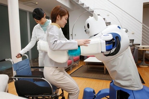
No commentsCould Pepper be the next technical genius?
The largest mobile phone operator in Japan, Softbank intends to sell robots they call “Pepper” in Japan in February 2015 and in the United States within a year through Sprint which they took control recently. Created by Aldebaran, the robot is priced at around $1,900. It is already greeting and welcoming customers at Softbank stores in Japan.
Pepper is an intelligent and first of its kind humanoid robot designed to live with humans. The social robot can recognize and react to your emotions and live without any assistance. Unfortunately it will not cook or clean for you. But he can be a good companion that reacts to your voice, touch and emotions. Pepper’s great ability is its reactions to your emotions. It can recognize your burst of laughter, your frown, anger, joy, sadness and translate that into its reaction. Analyses of your facial expressions, body language and words and adopting itself to cheer you up are Pepper’s sheer strength. He can play your favorite song for you no matter what the condition you are in. More you communicate with him, more data that he will gather to react and comfort you. What a companionship it will be?
No commentsMetal Finishing with Sputter Deposition
Written by: Denton Vacuum, LLC
Summary: Metallic finishes are applied using advanced manufacturing techniques.
Ever wonder how motorcycles, bicycles and cars all get that anodized finish to the metallic parts they use? Some of that work is old-fashioned elbow grease, but advanced manufacturing techniques like sputter deposition can help give metals the brushed finish hobbyists and collectors expect in high quality products.
Basic Technique
The piece to be finished is placed inside of a vacuum sealed chamber, where the process of plasma-enhanced chemical vapor deposition begins. The metallic coating of the substance is broken down into a gaseous form, using extremely intense heat. The molecules are then fed into a vacuum sealed chamber, which is cooled at precise intervals. As the chamber cools, the molecules come to settle upon the substrate. In order to form a smoother finish, the substrate may be rotated so the molecules can coat its surface evenly.
Using Magnets
Another method utilizes magnetron sputtering, which pulls and reflects particles based on their ionic charges. This technique is often used when an even coating is desired, because of how the molecules move within the chamber. Typically, magnetron sputtering systems leave no visible defects and the layers are microns in thickness.
Final Thoughts
There are a ton of uses for this technology that extend beyond the finish of hobby products. Plastics, for instance, can receive a metallic coating to reinforce their strength. That greatly reduces the costs of producing screws and other small objects needed in the construction of jet or car engines.
No commentsApplications for Thin Film Evaporation
Written by: Denton Vacuum, LLC
Summary: Thin film applies a smooth coating to a substrate, often changing its properties entirely.
Thin film evaporation allows manufacturers to coat devices with substances that can alter their properties entirely. This process is used in metallization of screws, where plastic pieces are turned into durable objects used in high-performance settings.
This manufacturing technique is used by many industries that produce products that live in your home.
Techniques
Thin Film is only one technique used to apply coatings to a substrate. In ion beam assisted coatings, a laser is used to guide the application of materials onto the substrate. Plasma-enhanced chemical vapor deposition superheats chemicals to a gas state, and is used in manufacturing solid objects like eye glasses.
Uses
To extend the eyeglass example, PECVD allows a manufacturer to break down a chemical into gaseous form. The molecules are applied to the lens as they cool, coming to settle on the surface of the lens as it is carefully rotated for an even coating. You may see this process at work in medical devices as well, especially in those that use hydrophilic coatings for better interaction with organic material.
Advantages to Thin Film
This technique is preferable to sputter deposition, because the finish created is smoother. It’s free from defects, or small inconsistencies that would normally coat an object that has undergone sputter deposition. It also makes it easier for manufacturers to bind certain chemicals and create entirely new substances. Plasma-enhanced silicon nitride, for example, is a thin film used in the formation of high performance automobile parts.
Related Story: How to Make a Semiconductor
Related Story: Handbook of Thin Film Devices
No commentsEquipping automobiles with chips
Newer cars are full of technology that does everything from detecting blind spots to automatic breaking. Models from Hyundai Motor are full of technology produced by many manufacturers. The automotive chip industry is expected to generate $27.9 billion this year and grow at a 6.1 percent per year. A new car carry more than $329 worth of semiconductors in each car and compare this to no more than $20 worth of semiconductors in an iPhone 5. The top suppliers of chips for automobile include Renesas Electronics, Infineon Technologies, STMicroelectronics, Denso, and Freescale Semiconductor. Intel, Qualcomm and Nvidia are trying hard to cut into the field and supply only very small amount at this time. Audi A7 uses Nvidia’s Tegra processor and Intel is making inroads with BMW, Nissan Motors and Hyundai.
Safety and reliability standards for chips in vehicles require far more compliance than computers and smartphones. Automobile chips require zero failure rate compared to 10 percent tolerance for electronics. Another difficulty is making chips that can withstand huge temperature fluctuations. Once installed, chips need to work for many years without having to replace constantly. Consumer expectations are also increasingly getting higher due to influence from other fast improving segments for higher speeds and power.
No commentsHow to Make Eye Glass Lenses
Eye glasses are made with very specific requirements in mind. The design and shape of the lens, as well as UHV sputter deposition coatings it may receive, contribute to the user’s overall visual quality. A lens that is shaped incorrectly, or one that is easily scratched, can quickly degrade a user’s vision and sometimes cause headaches and other side effects.
Cutting
First, the lens must be cut from a resin block called a lens blank. The size and shape is not unlike a hockey puck. The doctor dictates the cut of the lens, and gives a prescription that technicians translate into instructions for a computer. The lens is shaped according to those precise instructions, curving the front and back of the lens to bend light accordingly.
Fine Shaving
The lens is rough after this process, so the lens must be thoroughly polished. The lens is placed on a polishing block, where the convex end is rubbed with a fine grit to make it transparent. Of course, this is just the shaping and polishing of the lens. It must still be cut to size. A lens edger utilizes a diamond cutting wheel to trim the lens to the desired size.
Coating
Optical coating systems are used to add an anti-reflective coating to the lenses. The lenses are placed in a dust-free chamber, where they may receive up to sixteen separate layers of coatings designed to reduce scratches and glare. Some of these coatings even repel oil and water. Once the lens iscoated, it is fit to the glasses the customer ordered.
Related Story: Uses for Vacuum Evaporation
Related Story: Humanoid Robot Provides Inspection Service with a Smile
Bio: Denton Vacuum, LLC makes a thermal evaporation system for use in coating medical apparatuses. For medical manufacturing machinery, visit Denton Vacuum, LLC.
No commentsOLED technology to help TVs to get thinner and bigger
Introduction of curved TVs by Samsung, LG and others draw our attention to OLED (organic light-emitting diode) technology. OLED is different from traditional LED (light-emitting diode) because it uses organic substance that glows when electric current is introduced. The organic carbon-based compound emits its own light when treated with electrical current. A thin film transistors turn on and off of each pixel helping OLED to come up with thinner, lighter and higher resolution products such as TVs. The new material helps to reduce weight and thickness, and increase the size of TVs. When passes through filters it generates spectacular pictures for your viewing pleasure.
When compared to conventional cold cathode fluorescent lamp LCD (liquid crystal display) which requires backlight, OLED do not require a backlight and as a result pixels becomes truly black providing a higher contrast. Since elimination of backlighting layer, OLED hardware becomes thinner and lighter. The LED (light-emitting diode) also requires backlighting which is no longer required under OLED. OLED not just helps it to become thinner, it also provides a superior color reproduction due to pixels that turn on and off producing true blacks. The OLED technology also promotes energy efficiency over LCD and LED technologies.
No commentsMEMS Production Techniques
MEMS are built using materials that are not unlike those of a semiconductor. The microscopic machines require layers of materials that are built up, in precise patterns, to relay information or power from source to another. Using manufacturing techniques like plasma-enhanced chemical vapor distribution, materials can be arranged in precise patterns for carrying out complex operations.
Deposition
PECVD is part of the process that allows manufacturers to design objects within 100 micrometers. Gases are released onto a substrate, where they “grow” by layers as the gasses cool and adhere to one another. Essentially, materials are broken down and built up by layer. One of the methods used is sputtering, which uses a spray pattern not unlike a can of spray paint.
Lithography
The precise patterns used to create MEMS are only possible thanks to a process using thin film deposition. First, the object is coated in a lightly radioactive substance. This could be a beam of light, for instance. The exposed parts would differ from those that were not exposed, and then a machine deposits thin layers of materials onto the parts that light as touched.
Conclusions
Extreme precision makes it possible to create smaller mechanisms to handle a variety of everyday tasks in the house. MEMS help to gauge the stability of something, like a level, so you’ll often find them in video game and cell phone applications that display according to the orientation of the device.
Related Story: Optical Coating Systems for the Automotive Industry
Related Story: MEMS Technology to Drive Growth in Customization and Personalization
No commentsFlash to outshine disc-based storage
Spinning magnetic Disc-based storage mostly sold by HP, EMC, NetApp and many others are faced with a competition from flash. Toshiba invented the flash technology back in 1984. Chips stored data when the device even turned off and uses less energy, works faster and require less space. Memory cards and USB memory sticks started to use the technology first and around year 2000 much more uses were added to the roster. New chip technology allowed it to produce cheaper chips and allow it to store more data. This paved the way for flash chips to be used even in data centers. Sales of flash chips are expected to rise to $1.6 billion a year by 2016.
Some data centers faced with disc-storage limitations are switching over to flash. The popularity of data centers within last few years creates a steady demand for flash chip makers. This may be why traditional storage makers are acquiring startup flash chip manufacturers to get into the game. The disc-based storage leader EMC acquired three startups within last few years. With the number of flash makers entering the competition, prices of flash are seen lot of pressure and expected to go even further down.
No comments